PLATFORM TECHNOLOGY
Platform Technology
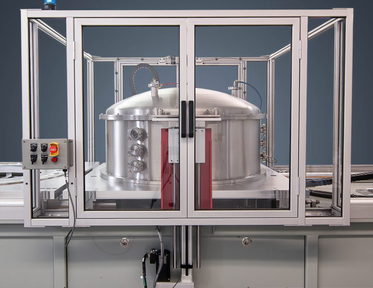
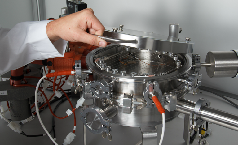
GVD’s platform technology is a polymer deposition process called Chemical Vapor Deposition (CVD), which produces high performance and high-quality films directly on the surface of the substrate from the vapor phase. In a single step, typically without exposing the product to high temperatures, solvents or other harsh processing conditions, our coating systems apply a nanometer or micron thin coating to enhance, protect, or prolong your process or product, using equipment and systems that enable repeatability & reproducibility. Most importantly, GVD has demonstrated CVD coating processes to be scalable, both, in terms of substrate size, and production volumes.
CVD technology rivals legacy solutions, such as wet-applied coatings. The latter are some of the most common surface modification approaches, typically applied via spray, dip, spin, or brush methods, both automatic and manual. The quality of the resulting coatings is highly dependent on operator skill and tools utilized for the coating process.
There are major advantages to using CVD:
There are no coverage concerns
The coating material deposited from the vapor phase builds in layers and creates a conformal and pinhole-free coating throughout any exposed part’s surface within the chamber. The resultant films deposit over complex and often high aspect ratio features, all without plugging cavities.
No coating migration occurs after application
A solid coating forms directly on unmasked surfaces, is fully polymerized upon deposition and does not require curing.
Coating process is repeatable and reproducible
Processing conditions (flow rate, pressure, etc.) are predetermined, set prior to each application using a recipe-based control system and are consistent run-to-run.
Coating thickness is controlled and verifiable
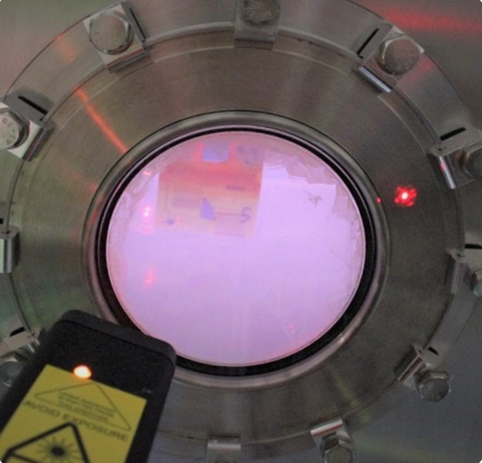
Coating thickness and deposition rate are monitored in-situ and in real-time using an interferometric technique on silicon witness wafers inserted in each batch. Additionally, thickness data is verified post deposition on witness wafers.

